Tips for designing a switching regulator (feat. TI LMR51450)
In this post I’m going to share some useful tips when designing a switching regulator, together with the considerations of picking up proper regulator ICs and other components.
As Texas Instruments has a wide category of power regulators, I am going to use the buck down converter LMR51450 as an example. The general rules can be applied to most of other switching regulators.
Selection of a proper regulator IC
The first thing is to note down the power requirements of your design, this should be done prior to looking for regulator ICs. Normally, the key considerations are input voltage, output voltage, output current, etc..
In this example, my design requirements are:
- Input voltage
V_IN: from 20V to 36V, with a nominal voltage of 24V. - Output voltage
V_OUT: 5V fixed, max. 5 % voltage ripple. - Output current
I_OUT: from 2A to 5A. - Efficiency: > 90%.
- Other: for compact design, low-cost, built-in protection …
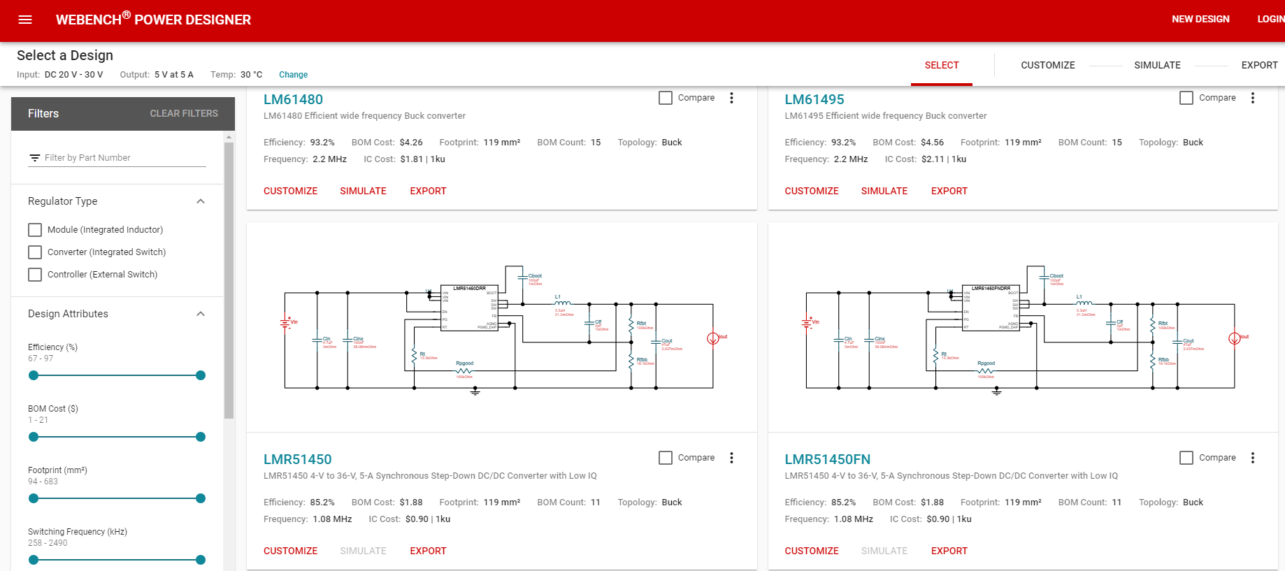
Depending on the above requirements, we can apply this as filters for components selection in Digi-key or Mouser to find suitable regulator ICs. However, if we just want to use products from Texas Instruments, we can use the WEBENCH POWER DESIGNER to quickly find the appropriate ICs from TI.
After giving my input in the WEBENCH designer, I quickly get the solutions from TI, I finally pick the LMR51450 as my solution.
Application circuit of LMR51450
The typical application circuit diagram for LMR51450 is shown below:
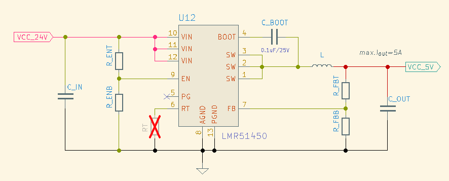
The detailed design procedure is described based on the above circuit.
Set the output voltage
The output voltage of LMR51450 is adjustable through the resistor divider on pin FB.
where \(V_{REF} = 0.8V\) to the datasheet.
To set the output voltage to 5V, choose \(R_{FBe}=100k\Omega\) and \(R_{FBB}=19.2k\Omega\).
Set the switching frequency
The switching frequency can be set by adjusting the value of \(R_{T}\) connected to the pin RT. If leave it open, the default switching frequency of LMR51450 is 500 kHz.
The higher switching frequency will:
-
✅allow for lower value inductors and smaller output capacitors, i.e. allows for using smaller footprint components and lower cost.
-
❌bring more switching loss, i.e. less efficient and generates more heat.
Select the inductor
The inductor plays an important role in a switching regulator, it does the job of:
- Energy Storage: it stores energy in its magnetic field when the switch is closed, and relases it when the switch is open.
- Output Smoothing: together with the capacitors, the pulsed source can be converted into a smooth DC to the load.
The most critical parameters for the inductor selection are the inductance, saturation current and RMS current.
Choose the right inductance
The inductance is based on the desired peak-to-peak ripple current \(\Delta i*{L}\). The minimum inductance \(L*{min}\) can be calculated using the following equation from datasheet:
\[L_{min} = \frac{V_{IN\_MAX} - V_{OUT}}{\Delta i_{L}}\times \frac{V_{OUT}}{V_{IN\_MAX}\times f_{SW}}\]where \(\Delta i_{L}\) is the output ripple current, and here we take it as 40% of max. output current.
For our design example, the min. inductor value is calculated to be 4.3 uH, choose a standard value of 4.7 uH or larger is fine.
In general choosing lower inductance is preferable because it usually correpsonds to faster transient response, smaller DCR and allows for more compact designs.
- If the inductance is too low, it can generate larger output current ripple, and thus cause more inductor core loss.
- If the inductance is too high, it can generate larger output voltage ripple with the same output capacitors.
Choose inductor current ratings
In general, the saturation current of the inductor must be higher than peak current of your design, which is \(i_{OUT} + \Delta i_{L}\). In our case, the saturation current must be greater than 7 A.
The RMS current of the inductor must be higher than the max. allowed current of the internal MOSFET in the converter IC, this can be refered from the IC datasheet. In our case, the RMS current must be greater than 9.6 A.
Based on the above considerations, the inductor PA4342.472NLT can be used in the example design.
Select the output capacitors
The output capacitors directly affect the steady state of output voltage ripple and stability. For the selection of output capacitors, the ESR and capacitance are the critical parameters to consider.
The maximum allowed ESR can be calculated by
\[ESR = \frac{\Delta V_{OUT\_ESR}}{\Delta i_{L}}\]In our case, assume \(\Delta V_{OUT\_ESR}\) same as the output voltage ripple (25 mV). Capacitors of ESR no larger than \(12.5 m\Omega\) should be considered.
The minimum required output capacitance can be calculated by using equation (13) from the datasheet, if the a large value of capacitance is required, use multiple smaller capacitors in parallel can reduce cost.
In our application, we use two 33uF/16V X7R ceramic capacitors.
Select the input capacitors
The input capacitors help stabilizing the input voltage and reducing noise. These should be placed as close as possible to the IC VIN pins.
There are following considerations for the input capacitors selection:
- The voltage rating must be greater than the max. input voltage. TI recommends a voltage rating of twice the max. input voltage.
- The typical recommended value for the high frequency decoupling is 10 uF or higher, ceramic capacitors have lower ESR and better performance for fast transient response. Use larger capacitors if the input has a higher voltage ripple.
- For high frequency decoupling, a 0.1 uF ceramic capacitor can be placed in parallel.
- If the input supply is located far from the IC, additional bulk capacitor can be placed in addition to the ceramic capacitors. Usually a 47 uF or 100 uF electrolytic capacitors is a good choice.
In our application, we use two 10uF/50V and one 0.1uF/50V ceramic capacitors.
Bootstrap capacitor
The bootstrap capacitor C_BOOT is used to provide the gate voltage of the high-side MOSFET to ensure it can be turned on properly. The bootstrap capacitor should be placed between pin SW and BOOT. TI recommends to use a 0.1 uF and rated at 16 V or higher ceramic capacitor.
Set UVLO
Setting a undervoltage lockout (UVLO) ensures that the device operates only when the supply voltage is within a safe range. It helps:
- Prevents Malfunction: UVLO prevents the device from turning on or continuing to operate if the voltage falls below the threshold we set.
- Avoids Brownouts: During a brownout condition (a temporary drop in voltage), UVLO can shut down the device to avoid improper operation and restart it when the voltage returns to a safe level.
The LMR51450 can activate the UVLO feature by a resistor divider network between pin EN and VIN. Refer to the equation (15) from the datasheet for the proper setting.
If UVLO feature is not required, simply connect EN to VIN, do not leave EN pin float.
Summary
Designing with a switching regulator includes the following steps:

The WEBENCH tool provides a convenient way to find the solutions with appropriate PMICs.
The selection of inductor and capacitors should be taken care of, because they are very critical for the efficiency and stabilization of the regulator. Follow the datasheet or application note for the PCB layout design.